Materials

Photovoltaics International Archive
Materials, Photovoltaics International Papers
An improved understanding of multicrystalline wafer quality can explain variations in cell performance across multicrystalline silicon blocks. Infrared scanning can detect precipitates in a silicon block, while photoluminescence combined with defect etching can reveal needle-like precipitates along the grain boundaries. Such precipitates typically lead to reduced shunt resistance. Crystallographic defects that lower the current collection and the final cell efficiency can also be identified. Understanding the influence of these defects is important for the development of a crystallisation technology that results in a substantially better cell efficiency. The use of the improved material quality in an innovative cell and module technology have led to the world record module efficiency of 17%. This paper will illustrate one example of how an improved understanding of multicrystalline wafer quality can explain the variations in cell performance.
Photovoltaics International Archive
Materials, Photovoltaics International Papers
Heat transfer and control of the temperature field are important in the production of silicon solar cell wafers. Present work focuses on the first steps of the production chain, i.e. crystallization and wafering. For the crystallization process, control of heat transfer is crucial for the ingot quality in terms of grain structure, impurity distribution, particle formation, and ingot stresses. Heat transfer is also important during subsequent processes, in particular the wire sawing of the silicon blocks into wafers. The paper emphasises the role of heat transfer and explains the consequences for these processes. Examples from experimental trials and measurements are combined with models and simulation methods.
Photovoltaics International Archive
Materials, Photovoltaics International Papers
With growth in 2009 suffering from recession and an ongoing credit crunch, this paper presents a review of the key trends in cell and module manufacture for the crystalline silicon (c-Si) PV module market. The c-Si segment remains the largest segment, and is competing effectively with less mature thin-film technologies. PV is still a largely uneconomic way to generate power, and requires subsidy to maintain sales volume and growth. While subsidies exist, the industry treads the narrow path of growing at a healthy clip, developing robust technology and business models, and mapping paths to profitable business without subsidies once PV installations become economically viable.
Photovoltaics International Archive
Materials, Photovoltaics International Papers
As polysilicon producers perform expansions and upgrades to increase production and improve operations, plant safety remains critical. Companies should routinely review their safety policies and effectively plan their projects to ensure uninterrupted product supply and create a safe environment for employees and the communities in which they operate. Both the design and the execution of expansion and upgrades to projects are critical as companies strive for minimal down time so that productivity is not affected. Such hazards and scenarios that may hinder and delay start-up, specifically in relation to polysilicon plants, are highlighted in this paper. Furthermore, the paper outlines how best to avoid these situations, offering methods of execution to achieve the three key measures of success: safety, high purity and minimal downtime.
Photovoltaics International Archive
Materials, Photovoltaics International Papers
The process of wafering silicon bricks into wafers represents about 20% of the entire production cost of crystalline silicon solar cells. In this paper, the basic principles and challenges of the wafering process are discussed. The multi-wire sawing technique used to manufacture wafers for crystalline silicon solar cells, with the reduction of kerf loss currently representing about 50% of the silicon, presents a major challenge for further research efforts. Another relevant field of research is the reduction of wafer thickness in order to obtain more wafers per millimetre of brick length. The last subject that is addressed in this paper is the general optimization of the wafer surface and geometry, as the multi-wire saw cutting process influences the mechanical properties of the wafers and can have further effects on subsequent process steps.
Photovoltaics International Archive
Materials, Photovoltaics International Papers
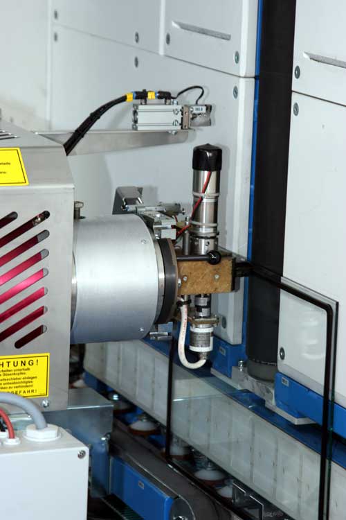
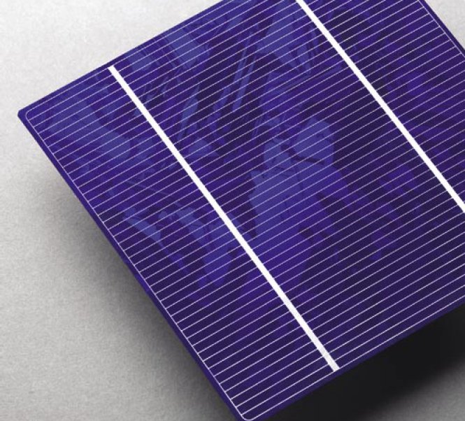
Although simple in concept, a photovoltaic solar cell is a difficult feat of technology in execution. The challenge of balancing cell structure design, material optimization and module technology to achieve efficient, low-cost modules that perform in aggressive environments for up to a generation is huge. The modules’ structure has to support and protect a thin, fragile slice of semiconductor, while ensuring a stable environment free from contamination and moisture with little or no change in the incident light on the cell. Key to the modules’ performance are the first-level polymeric materials that contact the cell and conductor structures, hold the module together, and in many cases form the second-level protection of the cells from the environment. In this article we explore the industry dynamics in the supply of advanced materials for module assembly, the new technology directions, and how the market will develop over the next five years.
Photovoltaics International Archive
Materials, Photovoltaics International Papers
Glass has been playing an ever more important role in photovoltaics, and with the increasing demand for solar modules, the glass industry will be pushed even more to the fore. As a result, the photovoltaics industry is fast becoming a field of business of increasing importance for some of the glass industry’s sectors. Mechanical engineering companies around the world are working to meet the demands of the solar industry, with the tremendous potential of glass, especially in the thin-film sector, at the epicentre of this effort. This paper presents the beneficial properties of glass for use in the photovoltaics industry, and the material’s potential for future applications.
Photovoltaics International Archive
Materials, Photovoltaics International Papers
Invented in their high efficiency version in the early 1990s, dye-sensitised solar cells (DSCs) entered the global market in 2007 with the first commercial modules based on this versatile, hybrid (organic-inorganic) technology. The 6-7% efficiency of the first modules is a result of their good performance in diffuse light conditions, allowing for the production of electricity both under cloudy conditions and indoors. These low-cost solar cells are manufactured by highly productive roll-to-roll printing methods over rigid or flexible substrates affording modules coloured in widely different tones. These attributes render DSC a photovoltaic technology particularly well suited for BIPV applications and for electrification in developing countries, as discussed in this paper.
Photovoltaics International Archive
Materials, Photovoltaics International Papers
Materials innovation in solar photovoltaic manufacturing has long played a key role in efforts to raise cell and module conversion efficiencies, improve overall device performance and reliability, and lower the overall cost per manufactured watt. Research and development in areas such as ultrathin-silicon wafering and replacement films for thin-film PV transparent conductive oxides often garner much of the industry’s attention. But a wide range of emerging technologies could provide crystalline-silicon and thin-film cell and module manufacturers the kinds of materials solutions that will accelerate their attempts to reach competitive levelized cost of energy metrics and ultimately attain their goal of achieving grid parity with conventional energy sources – as well as open up lucrative market opportunities for the materials suppliers.
Photovoltaics International Archive
Materials, Photovoltaics International Papers
A new wafer technology, named CDS (Crystallization on Dipped Substrate), is under development and has been found to be effective in the reduction of wafer cost and silicon feedstock. CDS technology was applied to 156mm x 156mm-sized wafers, obtained via the throughput of 1825cm2/min, and the resulting cell efficiency of 14.8% was confirmed. This paper outlines the principle behind the technology and outlines the procedure.

Subscribe to Newsletter

Most Read

Upcoming Events